Engineering the boards behind mission-critical electronics.
From simple prototypes to complex high-speed, multilayer, and rigid-flex designs — TMI Systems delivers production-ready PCB layouts on Cadence Allegro and Altium Designer. Concept to manufacturing. Zero compromises.

Design platforms & flows we master
End-to-end PCB design, delivered.
Every project starts with the engineer's intent and ends with a working, manufactured board. We handle every stage in between.
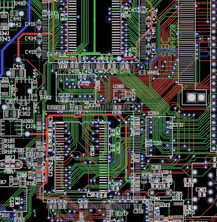
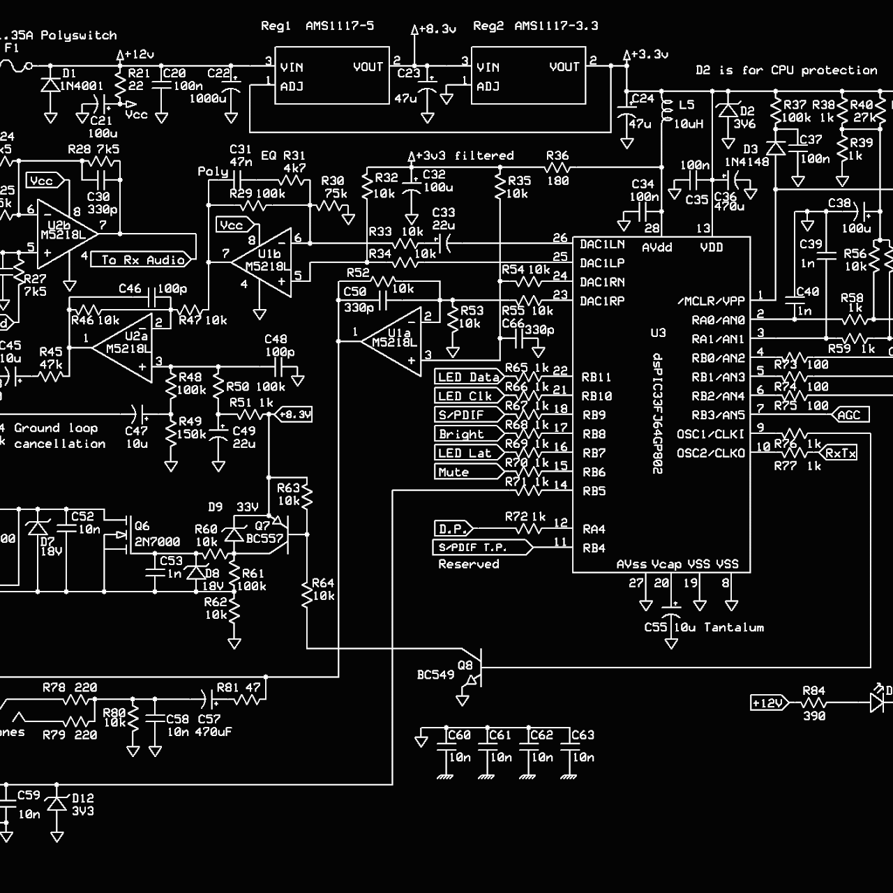
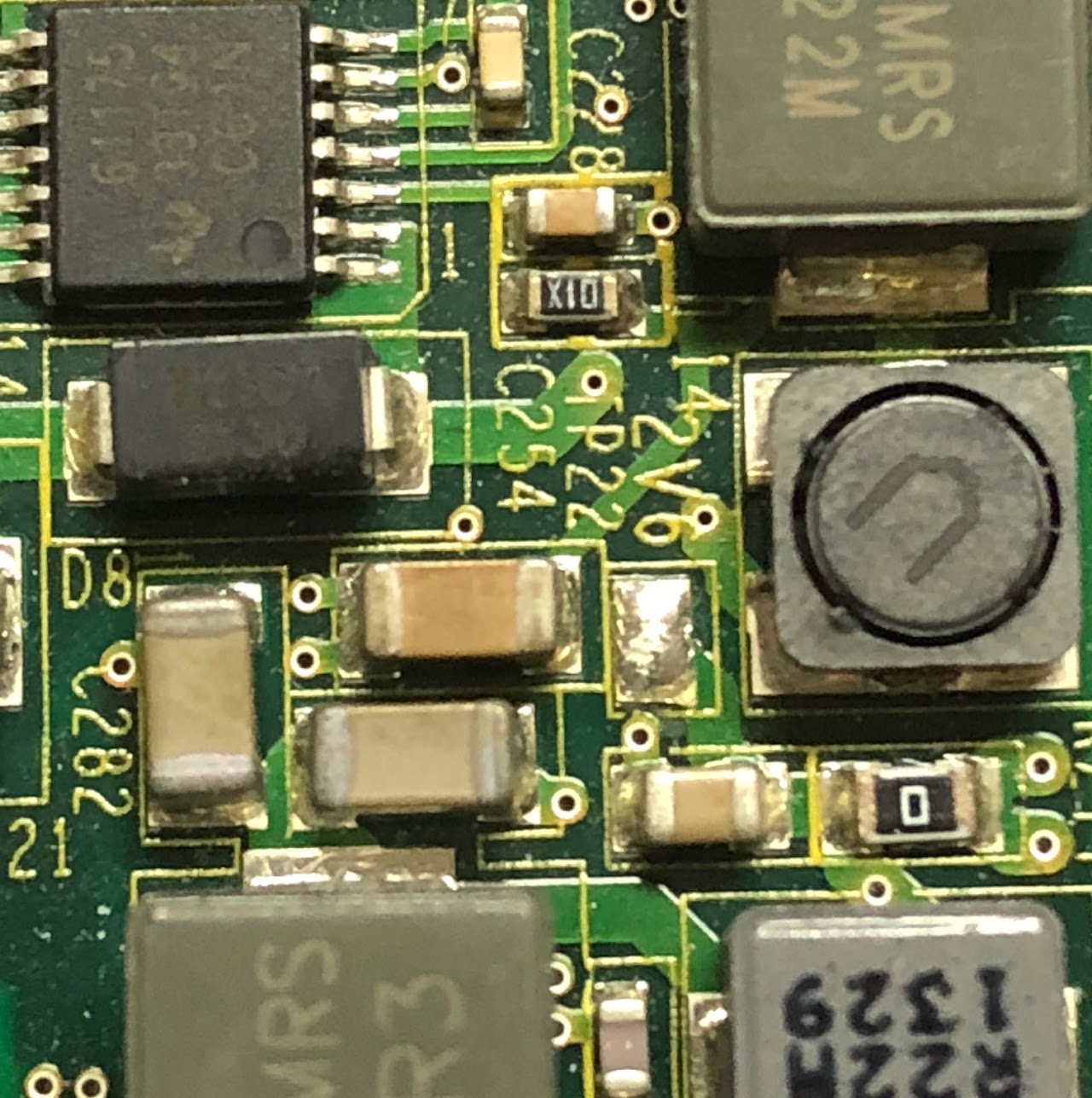
PCB Layout Design
Schematic-to-Gerber execution across the full complexity spectrum — simple prototypes to 20+ layer HDI stacks.
- High-speed digital & mixed-signal
- Rigid, flex, and rigid-flex
- HDI, backplane, heatsink boards
Signal & Power Integrity
Simulation-driven design for DDR4/5, PCIe Gen 4/5, USB, Ethernet, SerDes, and RF — where margin matters.
- Controlled impedance & differential pairs
- Length matching, crosstalk analysis
- Thermal & power plane optimization
Library Management
Custom footprints, symbols, and 3D STEP models built to a defined rule set — clean, consistent, and CAM-ready.
- IPC-7351 compliant footprints
- 3D STEP models for mechanical CAD
- Symbol & library migration
Manufacturing & Assembly
Turnkey production through vetted fabs in Europe, the US, and Asia. Competitive pricing, fastest lead times.
- Prototype & volume production
- SMT & mixed-technology assembly
- Testing, inspection, delivery
Rapid Prototyping
Quick-turn layout for engineers who need to validate fast. Short iteration cycles, clear communication.
- Same-day layout starts
- Revision-friendly workflows
- Parallel simulation & DFM
Design Consultancy
Pre-design reviews, constraint strategy, stack-up definition, and DFM feedback before a single trace is routed.
- Stack-up & impedance planning
- Component placement strategy
- DFM, DFA, and DFT reviews
Experience you can't shortcut.
Other bureaus learn on your board. We have 40+ years of completed projects, an ISO-certified process, and a team that has seen every edge case the physics of PCBs can throw at you.
Since 1986
Among the first PCB design houses in Israel. We've designed through every major generation of the industry.
95+ Active Customers
Repeat work from aerospace primes, medical device companies, defense contractors, and fabless silicon teams.
Tool-Agnostic Expertise
Cadence Allegro, Altium Designer, Mentor Xpedition, PADS — we deliver in the native format your team already uses.
By the Numbers
Where our boards ship.
From satellites in orbit to implanted medical devices — if the tolerance is tight and the stakes are high, our customers trust us with the layout.
Aerospace & Defense
Ruggedized designs, conformal-coat-friendly layouts, MIL-grade reliability.
Medical Devices
Implantables, diagnostic imaging, safety-critical monitoring.
Telecom & Networking
100G/400G backplanes, 5G front-end, SerDes-heavy designs.
Semiconductor & Test
Silicon validation boards, ATE fixtures, characterization platforms.
Industrial & IoT
Sensors, edge-compute, motor control, power conversion.
Consumer Electronics
Wearables, premium audio, rigid-flex mobile platforms.
Automotive
ADAS, infotainment, EV power electronics, AEC-Q conscious layout.
Energy & Power
High-current, high-voltage, thermal-heavy power boards.
Predictable workflow. Zero surprises.
Design review & constraint capture
We start by understanding the product, the schematic, the stack-up, and the critical interfaces. Constraints go in before placement begins.
Component placement & partitioning
Strategic placement for signal flow, thermal zones, EMI management, and mechanical compliance. Reviewed and approved before routing.
Constraint-driven routing
Impedance-controlled, length-matched, crosstalk-aware routing for high-speed interfaces. Power and ground handled with equal rigor.
Signal integrity & DFM checks
SI / PI / thermal simulation where the design demands it. DFM, DFA, and DFT validation against fab-specific rules.
Manufacturing data & handoff
Gerbers, ODB++, IPC-2581, drill files, assembly drawings, pick-and-place, BOM, STEP. Everything the fab and EMS need — nothing they don't.
Real boards. Real results.

Send us your schematic.
We'll send you back a plan.
Whether it's a quick-turn prototype or a 20-layer high-speed beast, we'll scope the work, quote it honestly, and hit the deadline.