Everything you need between schematic and shipment.
Full-service PCB design, simulation, library management, and turnkey manufacturing — under one roof, with a single point of accountability.
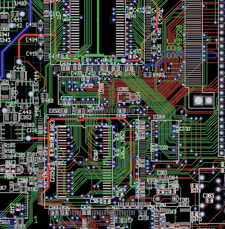
Layout that manufactures the first time.
From 2-layer prototypes to 24+ layer HDI high-speed beasts. We design boards that are routable, manufacturable, and testable — not just pretty in the CAD tool.
What's included
- Schematic review & design constraint capture
- Stack-up definition with fab-specific impedance
- Component placement & partitioning
- Constraint-driven routing
- Power & ground plane design
- DRC, DFM, and DFA sign-off
- Manufacturing & assembly data packages
Our layout process, start to finish.


Typical deliverables
- Pre-layout SI analysis & topology recommendations
- Post-layout signal integrity verification
- Power integrity / PDN impedance analysis
- Thermal simulation (board & component level)
- Crosstalk, reflection, and eye diagram reports
- Documented results & design recommendations
Margin you can measure.
For DDR4/5, PCIe Gen 4/5, 100/400GbE, USB 3.2/4, and SerDes above 25Gbps — spec sheets aren't enough. We simulate, verify, and document.
A library is a weapon.
Bad footprints kill boards. We build IPC-7351 compliant footprints, schematic symbols, and 3D STEP models against a defined rule set — then we maintain them.
Cadence Allegro, Altium Designer, Mentor Xpedition, PADS. Migrations between platforms. Centralized, version-controlled libraries that outlast individual designs.
Library services
- IPC-7351 compliant footprint creation
- Schematic symbol creation & standardization
- 3D STEP model generation
- Datasheet-driven validation
- Cross-tool library migration
- Ongoing maintenance & rule enforcement
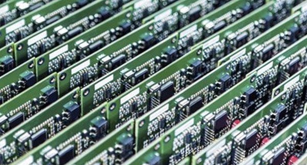
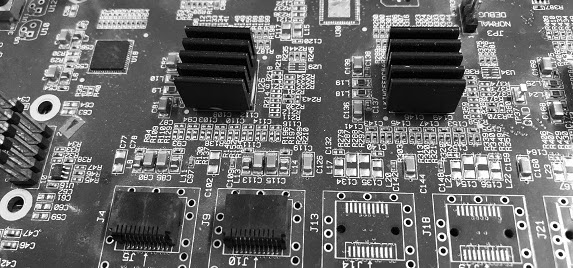
Manufacturing & Assembly
- PCB fabrication — prototype to production volume
- SMT, through-hole, and mixed-technology assembly
- BGA rework & fine-pitch placement
- Conformal coating & potting
- Functional testing & AOI inspection
- Global logistics & direct-to-customer delivery
One partner, working board at the end.
You send us a schematic. We return working, tested, boxed boards. Prototype or production. Vetted fabs in Europe, the US, and Asia. Competitive pricing, aggressive lead times.
Inside the manufacturing stack.


Specialized support when you need it.
Rapid Prototyping
Quick-turn layout for time-critical iterations. Same-day starts. Short revision cycles.
Design Consultancy
Pre-design reviews, stack-up planning, constraint strategy, DFM feedback before layout begins.
Format Migration
Allegro ↔ Altium ↔ Xpedition ↔ PADS. Faithful conversion of schematics, libraries, and PCB databases.
Design for Manufacture
Independent DFM, DFA, and DFT reviews on designs already in progress — catch issues before the fab does.
Stack-up & Impedance
Board stack-up definition, controlled-impedance calculation, fab-specific trace geometry engineering.
Legacy Board Support
Revitalizing older designs — PCAD 2006, Boardstation, old Allegro revisions. Keep mature products in production.
Not sure which service you need?
Send us your schematic, your constraints, or just your problem statement. We'll tell you exactly what the job requires.