Capabilities

If the physics allows it, we've routed it.

Every tool. Every technology. Every complexity class. Here's the full capability map — so you know exactly what we can take on.

Design Platforms

Native tool fluency — no conversion layer.

We work in your team's native CAD environment, maintain libraries in your format, and deliver in the exact file types your downstream workflow expects.

Cadence Allegro X

Full Allegro X Design Platform fluency — constraint-driven routing, high-speed analysis, PCB Editor Professional / High-End.

  • Constraint Manager expertise
  • High-speed & rigid-flex flows
  • Library migration & management

Altium Designer

Advanced Altium workflows — ActiveRoute, interactive routing, multi-board assemblies, Altium 365 collaboration.

  • Multi-channel & hierarchical designs
  • Rigid-flex stack-up editor
  • Version control & release management

Mentor Xpedition

Xpedition Enterprise / PADS Professional workflows for teams standardized on Siemens EDA.

  • xPCB Layout expertise
  • HyperLynx SI/PI integration
  • Variant & BOM management

PADS & Boardstation

Long-term support for teams on PADS or legacy Mentor Boardstation flows.

  • PADS Standard / Professional
  • Boardstation to modern EDA migration
  • Legacy board maintenance

Spectra & Auto-Routers

Cadence Allegro PCB Router (SPECROUTE), where auto-routing makes sense — and manual, where it doesn't.

  • Automated routing strategy
  • Constraint tuning
  • Hybrid automated + manual flow

Legacy & Niche

PCAD 2006, OrCAD, other older systems. We don't abandon mature products.

  • PCAD 2006 support
  • OrCAD capture & layout
  • Legacy migration paths
Board Technologies

Every substrate, every stack-up.

Construction Types

Rigid PCB Flex PCB Rigid-Flex HDI (μvia) Any-layer Backplane Heatsink / IMS Metal-core Thick-copper

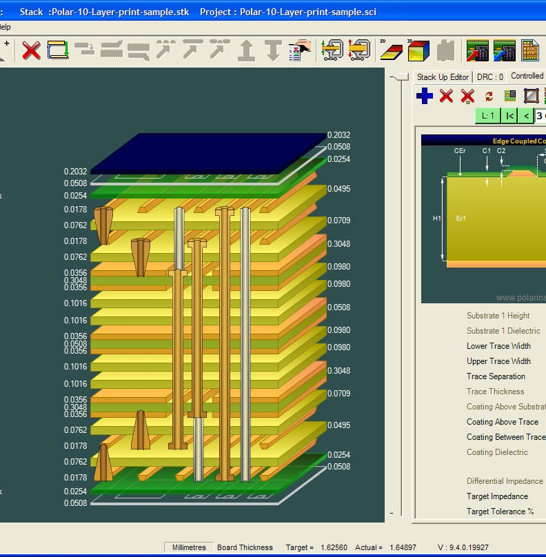
Layer Counts & Stack-ups

  • 2 to 24+ layer designs
  • Sequential lamination & blind/buried vias
  • Stacked & staggered microvias
  • Back-drilling for stub reduction
  • Impedance-controlled stack-ups
  • Mixed-dielectric (FR4 + high-speed + RF laminate)

Component & Package Types

BGA 0.3mm+ CSP QFN LGA POP 01005 passives Press-fit Press-fit connectors Embedded components

High-Speed Interfaces

  • DDR3 / DDR4 / DDR5 / LPDDR
  • PCIe Gen 3 / 4 / 5
  • USB 2.0 / 3.2 / USB4 / Thunderbolt
  • Ethernet 1G / 10G / 25G / 100G / 400G
  • SerDes interfaces (25–112 Gbps)
  • HDMI, DisplayPort, MIPI (CSI / DSI / D-PHY / C-PHY)
  • RF & microwave (to mmWave)
Standards & Compliance

Designs that pass audits, qual, and ECU review.

Layout standardsIPC-2221 / IPC-2222 / IPC-2223 (flex)
Footprint standardsIPC-7351 Generic Requirements
Qualification classesIPC Class 2 and Class 3
Acceptance criteriaIPC-A-600 / IPC-A-610
Manufacturing dataGerber X2, ODB++, IPC-2581
Company processISO-compliant PCB design workflow
TraceabilityFull version control & change history
Regulated-industry readyMedical, aerospace, defense documentation packages
Simulation & Analysis

We close the feedback loop.

Signal Integrity

Pre- and post-layout SI analysis, eye diagrams, crosstalk simulation, topology optimization for high-speed buses.

Signal integrity — waveform analysis

Power Integrity

PDN impedance analysis, decoupling strategy, IR-drop and transient analysis for power-hungry SoCs.

Power integrity — PDN analysis

Thermal

Board-level thermal simulation, copper pour strategy, heatsink integration, via-stitching for thermal paths.

Stack-up design and thermal planning
Simulation Workflow

Signal & Power Integrity simulation.

01 / 06
SIMULATION 01

Stack-up & Impedance Planning

Before a single trace is drawn, the stack-up is defined against the target fab's materials and capabilities — with impedance solved for every controlled-impedance net class.

  • Dielectric constants from fab data
  • Field solver for impedance
  • Plane-pair coupling for PDN
  • Layer count optimization
Stack-up & Impedance Planning
SIMULATION 02

Pre-Layout Topology Analysis

Topology simulation before routing begins — series termination, AC coupling, trace lengths, and receiver equalization planned from the schematic.

  • IBIS model extraction
  • Termination strategy optimization
  • Timing budget allocation
  • Pre-route feasibility check
Pre-Layout Topology Analysis
SIMULATION 03

Signal Integrity — Eye Diagrams

For 25Gbps+ SerDes, PCIe Gen 5, DDR5 and 400GbE, we run post-layout SI simulation and verify eye openings, jitter budgets, and link margin under worst-case PVT.

  • HFSS / SIwave extraction
  • Channel simulation with IBIS-AMI
  • Eye height / width / jitter verification
  • Loss, reflection, crosstalk budgets
Signal Integrity — Eye Diagrams
SIMULATION 04

Power Integrity — PDN Impedance

Decoupling strategy is solved, not guessed. We sweep the PDN impedance from DC to hundreds of MHz and size caps to keep the rail flat under transient load.

  • Target impedance from Icc & ripple
  • Cap selection & placement optimization
  • Plane resonance mitigation
  • IR-drop & current density maps
Power Integrity — PDN Impedance
SIMULATION 05

Crosstalk & EMI Analysis

Near-end and far-end crosstalk quantified. Radiated emission predicted against FCC/CISPR limits. Fixes applied in layout before hardware spin.

  • NEXT / FEXT simulation
  • Guard trace effectiveness
  • Radiated emission prediction
  • Shielding & filtering recommendations
Crosstalk & EMI Analysis
SIMULATION 06

Thermal Analysis

CFD and conduction simulation for boards with dense power stages or tightly packaged SoCs. We size copper, vias, and heatsinks before the thermal camera ever gets out.

  • Steady-state & transient thermal
  • Copper & via-farm optimization
  • Heatsink & enclosure coupling
  • Hotspot identification pre-fab
Thermal Analysis

Got a board we haven't listed?

If it's not here, ask anyway. 40 years of work means the edge cases tend to repeat.